Nuclear Weapons: NNSA Needs to Incorporate Additional Management Controls Over Its Microelectronics Activities
Fast Facts
Microelectronics used in nuclear weapons must function in environments with extremely high radiation levels. The National Nuclear Security Administration’s only source for producing these specialized microelectronics are aging facilities at Sandia National Labs.
NNSA is starting a $1 billion, 20-year effort to upgrade and sustain Sandia’s existing facilities and nuclear capabilities. NNSA has appointed a coordinator to lead this effort, but hasn’t fully developed a thorough set of controls for managing the cost, schedule, and associated risk. We recommended they develop such plans to effectively carry out planned microelectronics activities.
Microelectronics next to a U.S. dime
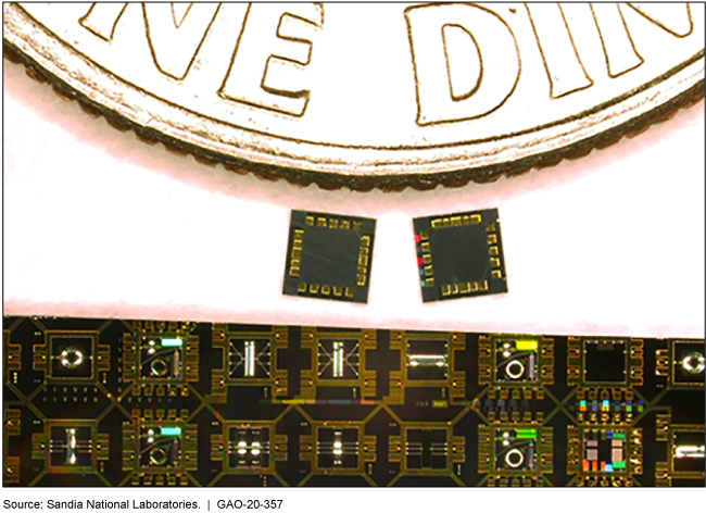
Tiny black shapes next to the edge of a dime
Highlights
What GAO Found
Over the past decade, the Department of Energy's (DOE) National Nuclear Security Administration (NNSA) completed several actions to sustain the condition of its existing microelectronics facilities at Sandia National Laboratories (Sandia), which are NNSA's only source for producing strategic radiation- hardened microelectronics that can operate in environments with extreme exposure to radiation. In particular, during fiscal years 2012 through 2019, NNSA carried out a multiyear, $150-million effort at Sandia to replace or refurbish infrastructure and equipment in its primary microelectronics production facility to ensure continued operations through 2025. While NNSA was working with Sandia to sustain current facilities, the agency also began identifying and evaluating options for producing microelectronics after 2025, including constructing a new multi-billion dollar production facility at Sandia. However, because of changes to key assumptions, including longer-term viability of existing facilities, NNSA decided in November 2018 not to pursue any of the identified alternatives and instead stated that the agency was going to assess options to sustain its current capability at Sandia.
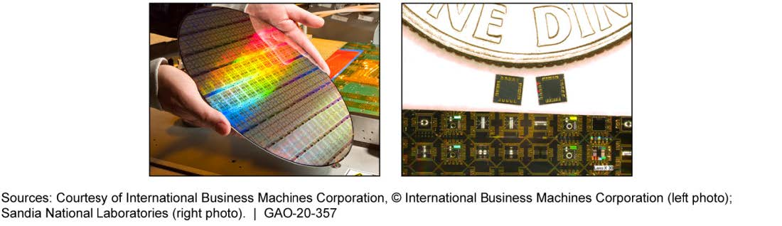
Photos of Microelectronics on a Silicon Wafer and Diced into Individual Parts
NNSA's ongoing approach to managing its strategic radiation-hardened microelectronics activities includes two key efforts. First, the agency decided in October 2019 to invest about $1 billion over the next 20 years to upgrade and sustain its microelectronics capability at Sandia through 2040. Specifically, NNSA plans to upgrade its production process as well as complete identified infrastructure (such as electrical distribution) and equipment projects. Second, in November 2019 NNSA created and filled a new full-time microelectronics coordinator position that, among other things, will have responsibility for certain aspects of the agency's microelectronics activities, according to agency officials. However, NNSA's approach does not fully incorporate key management controls that NNSA applies to other important activities. For example, DOE and NNSA require their programs and projects to establish an overarching management plan that describes the procedures to define, execute, and monitor a program or project as well as establishing specific requirements in a variety of areas such as cost estimating and performance management. NNSA has not established a similar management plan to oversee and coordinate its microelectronics activities. By incorporating these key management controls, NNSA would have increased assurance that its planned microelectronics activities are clearly defined, efficiently executed, and effectively monitored.
Why GAO Did This Study
Microelectronics (see figure) form the basis of nearly all electronic products, including nuclear weapons. U.S. nuclear weapons use a unique supply of “strategic radiation-hardened” microelectronics that must function properly when exposed to high levels of radiation. NNSA's facilities at Sandia are the only source for these unique microelectronics, and the age of the facilities may pose significant risk to NNSA's capability after 2025.
A Senate committee report accompanying the National Defense Authorization Act for Fiscal Year 2019 included a provision for GAO to review NNSA's strategic radiation- hardened microelectronics activities. This report (1) describes NNSA's actions over the past decade to sustain existing facilities and identify future alternatives; and (2) examines NNSA's ongoing approach to managing its microelectronics activities and the extent to which this approach incorporates key management controls. GAO reviewed documents and interviewed officials and contractor representatives from NNSA and Sandia, toured Sandia's microelectronics facilities, and reviewed NNSA program and project management controls.
Recommendations
GAO recommends that NNSA incorporate additional management controls, such as developing an overarching management plan, to better oversee and coordinate its microelectronics activities. NNSA neither agreed nor disagreed with this recommendation.
Recommendations for Executive Action
| Agency Affected | Recommendation | Status |
|---|---|---|
| National Nuclear Security Administration | The NNSA Administrator should incorporate additional management controls to better oversee and coordinate NNSA's microelectronics activities. Such management controls could include investing the microelectronics coordinator with increased responsibility and authority, developing an overarching management plan, and developing a mission need statement and a microelectronics requirements document. (Recommendation 1) |
NNSA has taken three key control actions to better oversee and coordinate its microelectronics activities. First, NNSA developed a set of integrated planning and execution documents. In 2020, NNSA issued two long-range planning documents: (1) an overall management plan that documented the roles, responsibilities, and anticipated funding support for four key program offices; and (2) a technology capabilities roadmap that identified seven areas where work activities will be focused. In September 2021, NNSA began issuing an annual implementation plan that provides specific direction on funding amounts and work activities. Second, NNSA increased the authority of the microelectronics coordinator, with the position now being classified at a program manager level. In addition, the microelectronics program manager is now responsible for preparing and issuing the annual implementation plan. Third, in fiscal year 2024, NNSA established a microelectronics working group, which according to agency documentation seeks to improve the coordination and communication between program manager and subject matter experts across headquarters, site offices, production plants, and laboratories. In addition, the working group is scheduled to complete an update of the 2020 technology capabilities roadmap by the end of fiscal year 2024. In total, these actions satisfy the intent of our recommendation.
|